Making Single Phase Solar Inverters Smaller, Cheaper, and Safer
Making Single Phase Solar Inverters Smaller, Cheaper, and Safer
ABSTRACT :
New technologies allow photo-voltaic (PV) inverters to switch at ever higher frequencies and consequently they are becoming much smaller and lighter. International competition and the move away from subsidies for new installations mean that there is strong pressure on their cost. The current transducers used in PV inverters must follow these trends: they must have a reduced footprint while having equivalent or improved performance at lower cost, compared to the transducers they replace. Typically PV installations use current transducers in three places. One is on the DC side, for the maximum power point tracking (MPPT) system. Two are on the AC side: first to define the parameters of the output current waveform, and secondly for safety reasons: for Residual Current Measurement (RCM) in the output caused by earth leakages, so the system may be closed down if necessary. This article shows how recently introduced LEM transducers can be used for MPPT and for AC waveform management, and then presents a new compact transducer specifically designed for RCM.
-
INTRODUCTION
Figure 1 shows main components around an inverter in a PV system typically used in residential installations of up to approximately 20kW. Several such inverters may be combined to make the complete installation which is connected to the grid via metering apparatus.

Figure 1. An inverter system for Photo-Voltaic installations.

Figure 2. Voltages and residual currents in the PV installation
During the last decade new silicon MOSFETs have been introduced in inverters, and in future MOSFETs based on SiC and GaN will begin to replace those using silicon. This is allowing higher frequency switching which in turn means that reactive components (inductors, capacitors) of lower value, and hence smaller physical dimensions, can be used. A 2kW inverter available in 2010 and weighing over 20 kg according to the manufacturer’s datasheet has been replaced in 2016 by a model weighing less than 10 kg. In order that the current transducers used as measurement devices in a PV system continue to use a negligible part of the overall space and weight budget, their size must also reduce without any performance degradation. Similarly their cost must reduce to follow the downwards cost trend of the complete inverter system.
There are 3 LEM current transducers in figure 1, all containing custom proprietary CMOS ASICs with fully integrated Hall cells. On the DC side of the inverter there is an open-loop GO; on the AC side a closed loop LPSR for the inverter control system and at the output an LDSR, a new differential transducer for RCM also with a closed loop architecture. (For a detailed explanation of Hall effect open and closed loop transducers see Reference (1)
Figure 2 shows the voltage waveforms on the DC and AC sides of the inverter. Note that in a transformer-less system, the “DC side” does indeed have a DC voltage corresponding to the output of the photovoltaic cells between the PV+ and PV- nodes (this may be increased by a DC-DC converter) but each of the PV nodes also has an AC voltage whose peak value is similar to the peak output voltage of the AC side. If not considered at the system level this represents a serious safety hazard.
-
CURRENT TRANSDUCERS IN THE PV INVERTER
2.1 The DC side.
Depending on the illumination intensity of the PV cells the load which maximizes the power transferred from them varies, and so the control system uses a real-time MPPT algorithm to load the cells for maximum power transfer. In the case of motorized PV panels the MPPT algorithm can also be used to obtain the optimum orientation. Since the target of the algorithm is simply to find the peak in the power transfer the accuracy requirement on the current transducer used is not demanding, and an open-loop transducer is ideal for this purpose. LEM has recently introduced the GO family of transducers (Reference (2)) which have the primary conductor integrated into a standard IC package. This gives a 70% PCB footprint reduction compared with a small transducer including a magnetic circuit. The SOIC-16 transducer is shown in figure 3. The principal specification parameters of the GO-SMS transducer in its SOIC-16 packaging are shown in Table 1.
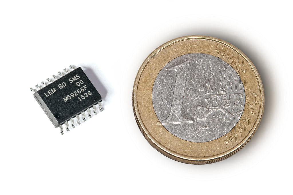
Figure 3: GO-SMS transducer in an SOIC-16 package
|
Parameter |
GO-SMS transducers |
|
Nominal current range (A) |
10 – 30 |
|
External field immunity |
Yes: gradient sensor |
|
Insulation test, 50 Hz, 1 min (kV) |
3 |
|
Impulse test voltage, 50 us (kV) |
4 |
|
Creepage, clearance distances (mm) |
7.5 |
|
Accuracy over 25 - 105°C (%) |
3.25 |
|
Primary resistance (mW) |
0.75 |
|
Out-of-range detection |
Yes, 10 ms response time |
|
Short-circuit detection |
Yes, 2.1 ms response time |
|
Response time ms |
<2 |
|
Offset drift (10 A model) (mA/K) |
0.94 |
|
Sensitivity drift (ppm/K) |
150 |
|
Magnetic offset |
0 |
|
Footprint (mm2) |
100 |
Table 1. Main performances of the GO-SMS transducer
The accuracy of the GO transducers exceeds that which is needed for the MPPT algorithm, and they may also be used at system level for other purposes, for example by comparing the outputs of different PV panels receiving similar illumination to identify faulty panels.
2.2 The AC side.
The transducer shown after the inverter in figure 1 is a key element of the control loop which drives the inverter switches and so governs the accuracy of the current output waveform. It must have a fast response time, low noise and good linearity, and in particular the offset and its drift with temperature must be low so that the DC component of the current injected into the grid meets regulatory requirements. Closed-loop transducers have an architecture which, due to the transformer effect, give good speed, noise and linearity performance. Historically the low offset requirements have been met using a fluxgate as the magnetically sensitive element. However low offset (and low offset drift) are now achieved by design innovations in the CMOS ASIC used in, for example, the LPSR family of transducers. The ASIC includes Hall cells and low offset amplifiers merged in a new patented architecture which allows the input related offset drift of the sensor to be around 4ppm/°C (25 A model). The result is a sensor whose construction is simpler than that of the fluxgate families with similar performance. Table 2 summarizes the key performance parameters. The LPSR family of transducers has been described in detail in Reference (3).
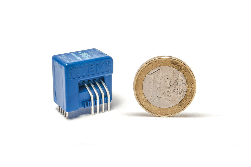
Figure 4: LPSR current transducer with an ASIC using the Hall effect Closed Loop technology
|
Parameter |
LPSR 25-NP |
|
Sensitivity error (%) |
+/-0.2 |
|
Temperature coefficient of sensitivity (ppm/°C) |
+/- 40 |
|
Electrical offset voltage (mV) |
+/- 1 |
|
Magnetic offset current (mA) after overload 10 x IPN (Referred to primary) |
+/- 60 |
|
Reference Voltage VREF @ IP = 0 |
2.485 – 2.515 |
|
Temperature coefficient of VREF @ IP = 0 (ppm/°C of 2.5 V) |
+/- 70 |
|
Temperature coefficient of VOUT @ IP = 0 (ppm/°C of 2.5 V) |
+/- 4 |
|
Linearity (%) |
+/- 0.1 |
|
Response time @ 90 % of IPN step (ns) |
400 |
|
Overall accuracy (% of IPN) @ 25°C |
0.8 |
|
Overall accuracy @ TA=85°C (% of IPN) |
0.85 |
|
Overall accuracy @ TA=105°C (% of IPN) |
0.9 |
Table 2. Main performances of LPSR 25-NP
2.3 Residual Current Measurement for Safety.
The nodes PV+ and PV- of figure 1 are physically large in a typical PV system. The average voltage on each node, relative to ground, is half of the voltage from the PV cells but on this is added an AC voltage whose peak-peak value is similar to that of the cells. In the event of a person touching the PV+ or PV- nodes (or, in general, any node on the DC side of the inverter) a leakage current will flow out of the system through the person to ground. Since there is only one node in the system whose potential is maintained at ground level, the N node at the output, this leakage must flow back into the system through the N node, and this will cause a DC current imbalance, or residual current, between the L and N outputs. This residual current must be detected, permitting the system to take very fast action to protect the person who has caused the residual current to flow. Among the challenges in RCM are:
- The absolute value of the current to be detected is low, some 10’s of mA, and so the transducer offsets must be low enough for this level of current to be detected;
- The AC current at the output is between zero and 10’s of A, and the residual current must be detected in the presence of this;
- Capacitance between the PV panels and ground mean that there is always some current flowing to ground, and the system objective is to distinguish these from an extra current caused by dangerous human contact.
Figure 2 shows the leakage current path in a simplified inverter system with the new LEM LDSR transducer used for RCM.
Of the three challenges listed, (i) and (ii) have been achieved in the LDSR by a special transducer design dedicated to RCM, while (iii) is achieved by applying a signal processing algorithm to the transducer output.
Figure 5 shows the principal of RCM: a Hall cell ASIC similar to that used in the LPSR example presented above is the heart of a closed-loop transducer. The AC currents I1 and I2 cancel, and the low residual current is detected by the Hall cell ASIC and compensated by a secondary winding having far fewer turns than in the case of the LPSR, since the current to be detected is much lower.

Figure 5: RCM operation principle based on the Hall effect closed loop technology.
Detailed analyses of the effect of the position of the primary conductors in figure 5 shows that the cancellation of I1 and I2 is not perfect and the residual magnetic field in the air gap depends on their position. Therefore it was decided to define the primary positions exactly by placing them on a multi-layer PCB inside the transducer. Furthermore, for RCM only a few dozen turns are required for the secondary coil, which means they can also be written on a PCB. In this way an innovative sensor has been designed whose construction is far simpler than that of earlier sensors. Having the primary conductors on a PCB limits the maximum primary current, but the allowed value of 35 A in each conductor is more than enough for domestic installations.
With primary currents of this value the design of the PCB on which the LDSR is mounted is important. Simulations have shown that with an optimized design the temperature rise in the transducer due to a 35 A primary current is limited to 13 oC

Figure 6. The LDSR transducer with planar primary conductors and magnetic core.
Figure 6 shows a simplified drawing of the LDSR transducer with its package removed. For test purposes an additional coil is wound on the ASIC PCB concentrically with the secondary circuit. This is useful for a system test: a current passed through it will give a transducer output in the same way as the current difference between the primaries.
Figure 6 shows a transducer with a single primary phase, it is also available with three phases.
As with the LPSR transducer the ASIC is designed for minimum offset, and the offset referred back to the input current is reduced by placing a hole in the PCB under the ASIC, allowing the smallest possible air gap in the magnetic circuit.
Because of the high sensitivity of the LDSR a magnetic shield (not shown in figure 6, for clarity) is placed around the ASIC and air gap.
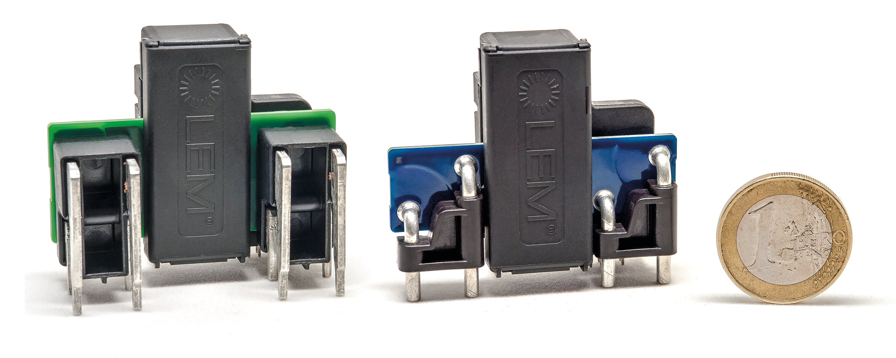
Figure 7 shows a photograph of the LDSR transducer.

Figure 7. LDSR in single and three phase versions.
|
Parameter |
LDSR 0.3-TP |
|
Sensitivity error (%) |
+/-2 |
|
Temperature coefficient of sensitivity (ppm/°C) |
+/- 250 |
|
Accuracy (mA) without initial offset @ from -40 to +105°C |
+/-40 |
|
Accuracy (mA) without initial offset @ 30 mA for +/-30 mA instantaneous DC jump |
+/- 8 |
|
Accuracy (mA) without initial offset @ 60 mA for +/-60 mA instantaneous DC jump |
+/- 12 |
|
Accuracy (mA) without initial offset @ 150 mA for +/-150 mA instantaneous DC jump |
+/- 20 |
|
Reference Voltage VREF @ IPRN = 0 |
2.485 – 2.515 |
|
Response time @ 90 % of IPRN step (us) |
300 |
Table 3. Main performances of LDSR 0.3-TP
In general the leakage currents detected by the LDSR will have an AC and a DC component and each user will use a specific algorithm on the transducer output to determine when a leakage is ‘excessive’ and take appropriate action. A particularly challenging case occurs when there is a large natural and variable AC leakage component (depending on ambient humidity, for example) through parasitic capacitances and the extra leakage caused by a person touching the DC side must be detected. The impedance presented by a person is largely resistive, and so, as shown in Figure 8, the extra current flowing makes almost no difference to the RMS value of the leakage current; the main effect is a change of phase.
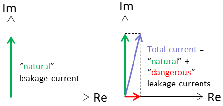
Figure 8: The effect of adding a resistive path to the leakage
In general of course there is also noise which adds to the real and imaginary currents of figure 8. In a case where only one known frequency must be analysed in a sampled waveform the Goertzel algorithm is particularly efficient. In figure 9 a 30mA rms ‘person leakage’ current is added to a 300mA rms ‘capacitive leakage’ current with 7.5mArms of noise at time = 0.1 s. The visible effect on the total leakage current is quite invisible, but after treatment with the Goertzel algorithm the 30mA current step is easily recovered and if this value exceeds a predefined threshold value appropriate action can be taken at the system level.

Figure 9. Simulation of residual current during fault and output of the Goertzel algorithm.
Conclusion.
This paper has used the example of photovoltaic installations to show the advances in recent LEM current transducers. Their size and cost are reducing while performance is maintained or improved. Transducers are now designed without the magnetic circuit or fluxgate component previously needed. This innovation is enabled by moving the complexity of transducer design into the custom Hall effect ASICs they use.
Written by LEM SA
Reference (1): https://www.lem.com/en/file/3139/download
Reference (2): Bodo’s Power Systems April 2017 issue “A New Family of Miniature, Fast and Accurate Transducers for Isolated Current Measurement”
Reference (3): Bodo’s Power Systems May 2017 issue “Closed Loop Current Transducers with Excellent Performance are also Cost-Effective”

